-
Notifications
You must be signed in to change notification settings - Fork 13
Memory Wall
In the HPC community the term Memory Wall was used in the late nineties to describe the situation where flops are cheap and main memory bandwidth is precious and scarce. The narrative was, that it is much easier to increase the instruction throughput of a processor architecture than its main memory bandwidth. As we all know things went different and while there is a gap between instruction throughput and memory bandwidth capabilities it is for sure not dramatically opening.
The view on processor architectures at that time was influenced by the fact that most application codes where classical numerical codes which are in most cases limited by main memory bandwidth. The impression was that engineers built processors no one (well at least no one in the HPC community) could fully exploit. Today the HPC application landscape is more diverse and multiple applications are making full use of the instruction throughput capabilities of processors, e.g., in the molecular dynamics domain.
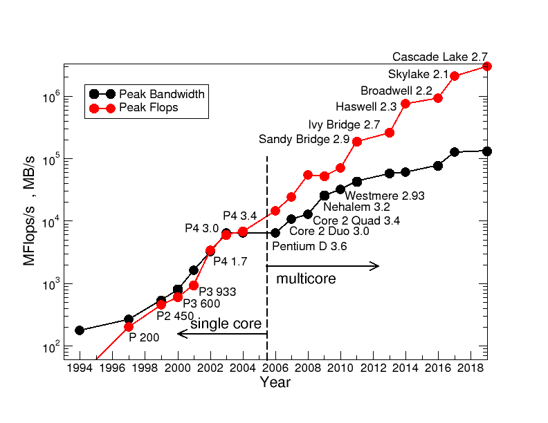
Lets look at real data to investigate how the memory wall developed over time. The following graph shows peak memory bandwidth (black line) and peak double precision flop rates (red line) for one socket of Intel server chips over 35 years. The y-axis (MB/s for the bandwidth and MFlops/s for peak performance) is in logarithmic scale! The dashed vertical line separates processors of the single-core and multi-core eras. The number behind the processor micro-architecture is the frequency. We choose top bin variants for every generation. Because modern processors run with various frequencies we choose the applicable scalar or SIMD Turbo frequency.

Starting with the multi-core era a gap is opening between peak performance and main memory bandwidth. Bumps in performance occur for Pentium 4, SandyBridge, Haswell and Skylake. Those processors introduced new processor features: Data parallel processing (16b-wide SSE, 32b-wide AVX, and 64b-wide AVX512) and fused-multiply add instructions (a one time stunt added in Haswell processors).
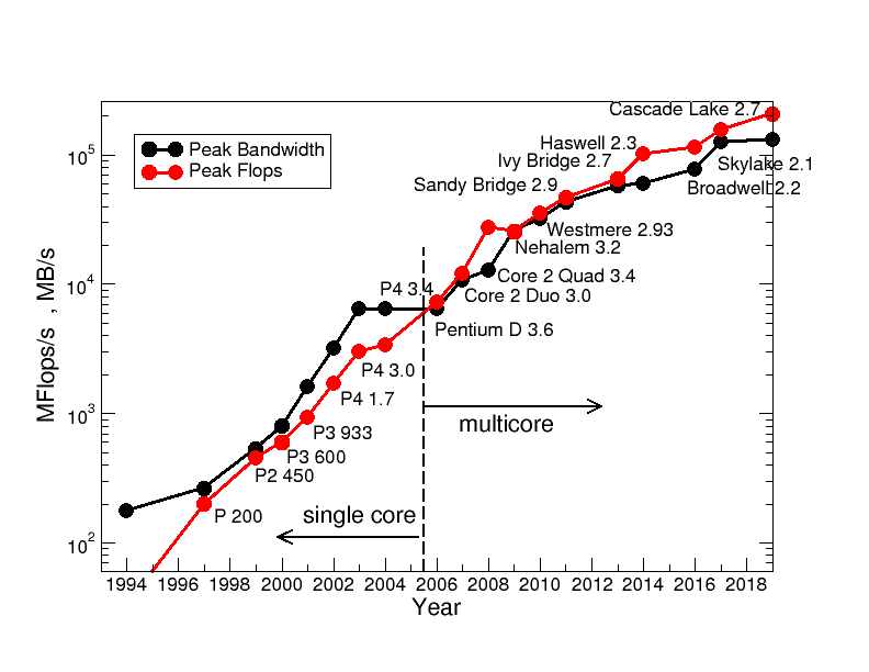
Lets look at this plot again for scalar code not using the new features. Now the performance is solely driven by the product of the number of cores, frequency, and superscalar execution.

No gap opens anymore! The peak performance and the memory bandwidth develop in parallel over the years. What about all the cores added? And there we are at a new wall processor architecture is facing: The power wall. Processors are sophisticated heating plates, the performance limit is governed by the total heat you can dissipate across the tiny die surface. Due to this limitation hardware architects trade used cores for frequency, from 3.6 GHz in Pentium D to 2 GHz nowadays. You have to give engineers credit for dynamically giving you a higher frequency if not using all cores. A feature called Turbo mode. To achieve a performance increase the engineers silently increased the TDP (Thermal design power) from 96W in Nehalem to 205W in Cascadelake. Despite these efforts the performance levels off lately compared to the single core era where performance was mainly driven by huge frequency increases. The memory bandwidth was also significantly increased over the years by adding more memory channels, but also by increasing the memory clock. With standard DRAM technology you achieve more than 150GB/s on one socket. And with High Bandwidth Memory (HBM) used in some HPC chips (e.g., NEC Aurora and Fujitsu A64FX) 1 TB/s and more is possible. The next years will show what engineers have to offer to drive chip and socket performance even further.