-
Notifications
You must be signed in to change notification settings - Fork 6
NuLA Adapter
Nula Adapter Installation
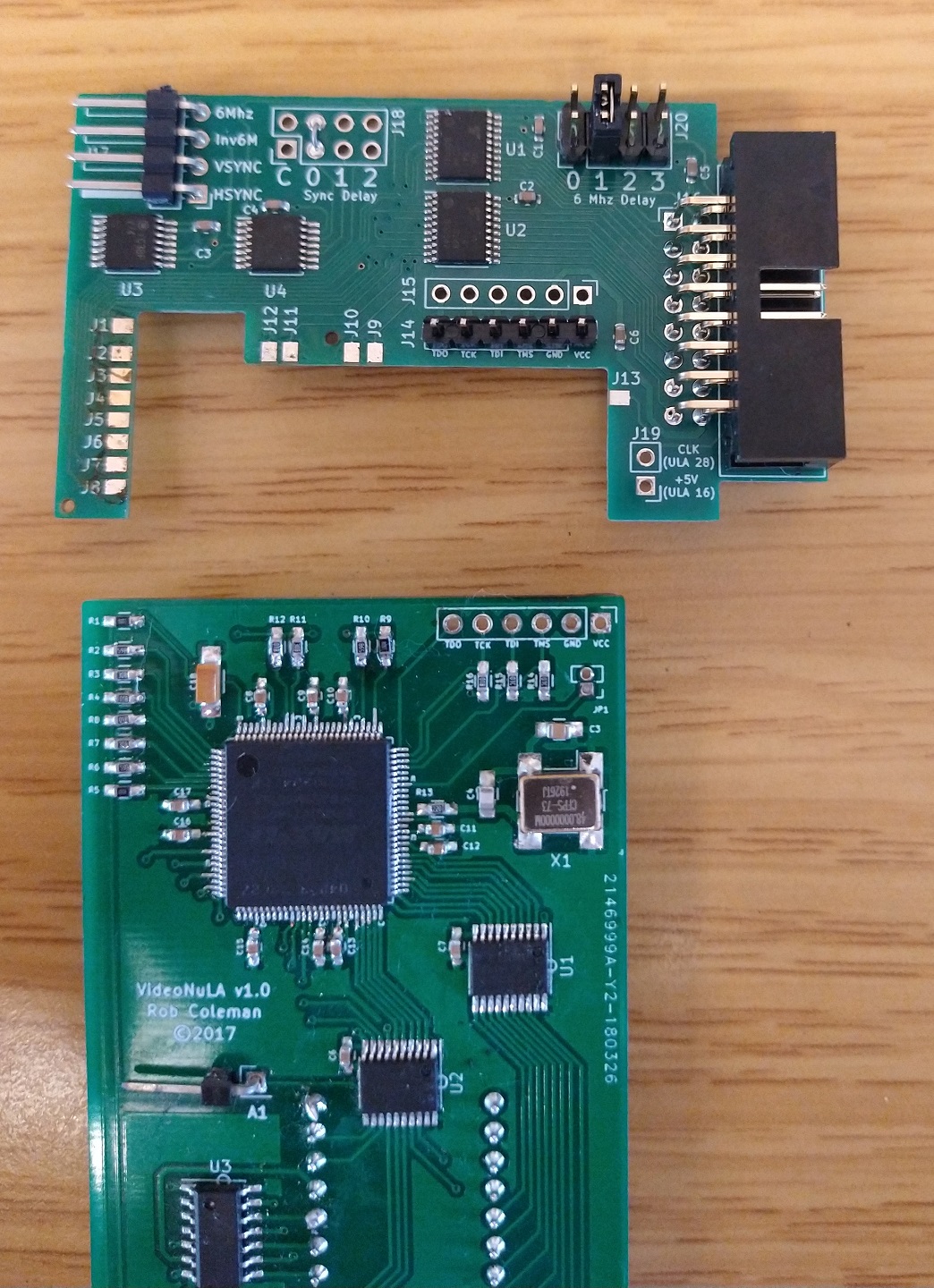
Push the pin header J14 of the adapter into the JTAG holes on the NuLA

Only solder the GND pin (2nd from edge) as soldering multiple pins will make it very difficult to remove if required

Heat up the GND pin with a soldering iron and adjust the adapter board until it is lying flat on top of the resistors with just their ends visible

Solder wire jumpers from each resistor end to J1 - J12

Solder a wire jumper from JP1 on the NuLA to J13 on the adapter

Solder the wires to the ULA header pins 16 and 28

Connect the Hsync and Vsync outputs of the 6845 (Pin 39 = Hsync, Pin 40 = Vsync) to the adapter Isolate Pin 19 (TR6) of the SAA5050 by either cutting and bending it out, cutting the pcb track or cutting the pin of the TTL chip connected to it Connect the 6Mhz out to pin Pin 19 of the SAA5050 Alternatively connect the Inv6M which is the inverted version of the 6Mhz
Jumpers The Sync jumper setting allows 0, 1 or 2 gate delays (default 0 delay) The "C" setting is Composite bypass which bypasses the sync regenerator and uses the BBC composite sync fed to the hsync input The 6Mhz delay jumpers allow 0, 2, 3 or 3 gate delays (default 1 delay)
Construction (current designs)
- Bill of Materials (12-Bit Board)
- Bill of Materials (12-Bit Extender)
- Bill of Materials (Analog Board)
- Bill of Materials (TTL Buffer Boards)
- Bill of Materials (Pi Zero)
- Cables
- Assembled boards for sale
Construction (older designs)
- Bill of Materials (6/8-Bit Board)
- Bill of Materials (6-Bit Board)
- Bill of Materials (3-Bit Board)
- Bill of Materials (Atom Board)
- Assembly Notes (Atom Board)
- CPLD Programming
User Documentation