-
Notifications
You must be signed in to change notification settings - Fork 6
NuLA Adapter
Nula Adapter Installation
Before starting, check that 6Mhz is being output on JP1 of the Nula (near the JTAG header)
If that isn't being generated, contact RobC for a firmware update (see: https://stardot.org.uk/forums/viewtopic.php?p=427323#p427323 ) or consider using the clock fixer to generate an alternative 6Mhz
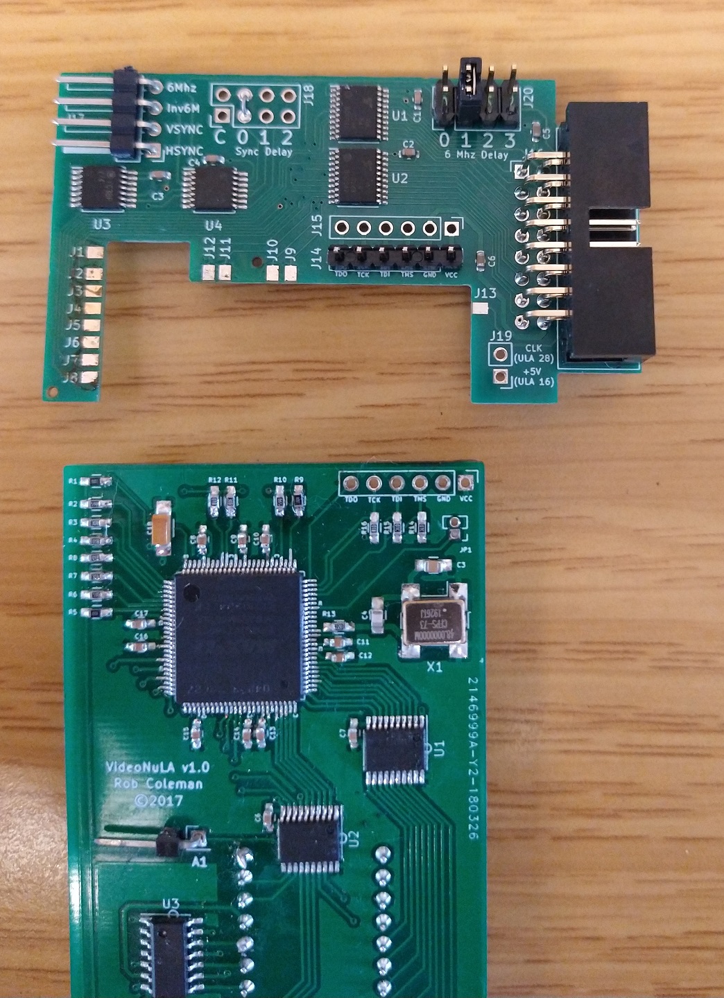
Push the pin header J14 of the adapter into the JTAG holes on the NuLA

Only solder the GND pin (2nd from edge) as soldering multiple pins will make it very difficult to remove if required
The other pins are only used for JTAG reprogramming

Heat up the GND pin with a soldering iron and adjust the adapter board until it is lying flat on top of the resistors with just their ends visible

Solder wire jumpers from each resistor end to J1 - J12

Solder a wire jumper from JP1 on the NuLA to J13 on the adapter

Solder the wires to the ULA header pins 16 and 28

Pick up the Hsync and Vsync outputs of the 6845 (Pin 39 = Hsync, Pin 40 = Vsync) and connect them to the adapter using dupont cables. You can solder one end to the 6845 pins and plug the other end into the HSYNC and VSYNC inputs on the adapter board. (Do not modify or cut the 6845 pins)
The new 6Mhz from the adapter has to be connected to the SAA5050 replacing the original 6Mhz and there are several ways to do this:
Option A: The most direct way is to isolate Pin 19 (TR6) of the SAA5050 by either by bending it out if socketed or cutting and bending it out if soldered and then plug one end of the dupont cable into the 6Mhz out of the adapter and solder the other end to the bent out Pin 19 of the SAA5050.
Option B: Cut the pin of the chip connected to Pin 19 (TR6) of the SAA5050 and then plug one end of the dupont cable into the 6Mhz out of the adapter and solder the other end to Pin 19 of the SAA5050.
Cut IC37 (74LS04) pin 8 for the BBC to isolate Pin 19 on the SAA5050
Cut IC25 (74LS86) pin 11 for the Master to isolate Pin 19 on the SAA5050
Option C (Not recommended due to thermal drift):
Remove a resistor and capacitor to disconnect the existing 6Mhz signal and connect the 6Mhz out of the adapter at that point:
For the BBC:
Remove R119 (100R) and C48 (270pF) and solder the 6 Mhz cable to IC37 (74LS04) pin 9
For the Master:
Remove R59 (150R) and C30 (100pf) and solder the 6 Mhz cable to IC25 (74LS86) pin 12
You could just lift one leg and leave one leg of the above resistors and capacitors in the board so it would easy to undo.
To understand what these changes do, find the SAA5050 on the relevant schematic and follow the connection back from pin 19 until you find those chips.
Note Option C passes the new 6Mhz through a TTL chip before connecting to the SAA5050 and that will likely cause thermal drift in the calibration so you will have to try one of the other options if that happens.
Jumpers
The Sync jumper setting allows 0, 1 or 2 gate delays (default 0 delay)
The "C" setting is Composite bypass which bypasses the sync regenerator and uses the BBC composite sync fed to the hsync input
The 6Mhz delay jumpers allow 0, 1, 2 or 3 gate delays (default 1 delay)
Usage
Connect the NuLA adapter to an RGBtoHDMI with a 12 bit extender fitted using a 16 way ribbon cable.
Select one of the NuLA profiles in the BBC CPLD
The NuLA 3bpp Mode7 profiles don't show the extra NuLA colours in mode7 but use the high quality mode7 deinterlacing.
The NuLA 12bpp Mode7 profiles will show the extra NuLA colours in mode7 but only use weave deinterlacing in mode7.
For each profile, run the auto calibration in mode 7, preferably using the mode7 calibration test pattern and also mode 0, then save the results.
After that you would only need to run the calibration again after a software upgrade.
A mode 7 calibration test program can be downloaded here: https://raw.githubusercontent.com/wiki/hoglet67/RGBtoHDMI/images/Mode7_Calibration.zip
If you have problems getting a clean calibration then try adjusting the 6Mhz delay jumper or try moving the 6Mhz cable to the Inverted 6Mhz pin (Inv6M)
Testing
Use *VNPALETTE to start the palette programming menu and use R and Shift R then G and Shift G then B and Shift B to step up and down the 16 possible levels to confirm they are displayed correctly.
If you are happy that everything is working and reliable after several days testing, you can solder the remaining JTAG pins for extra mechanical strength and that will also allow reprogramming via J15 but it will be very difficult to remove after that. (To remove after fully soldering you would need to heat and remove each pin individually and then use hot air to separate the two boards as they are so close together the pads will be connected with solder blobs)
Construction (current designs)
- Bill of Materials (12-Bit Board)
- Bill of Materials (12-Bit Extender)
- Bill of Materials (Analog Board)
- Bill of Materials (TTL Buffer Boards)
- Bill of Materials (Pi Zero)
- Cables
- Assembled boards for sale
Construction (older designs)
- Bill of Materials (6/8-Bit Board)
- Bill of Materials (6-Bit Board)
- Bill of Materials (3-Bit Board)
- Bill of Materials (Atom Board)
- Assembly Notes (Atom Board)
- CPLD Programming
User Documentation